
Loongson used to make CPUs based off the MIPS ISA, but the company recently switched to a homegrown ISA called Loongarch. This “new” ISA retains many of MIPS’s semantics, but uses incompatible encodings. Loongarch also gets extended to better support Loongson’s goals of making a viable domestic Chinese CPU.
Loongarch’s LSX and LASX vector extensions are a prominent example of this. LSX is a bit like SSE on x86, with 128-bit vector registers and corresponding instructions. LASX can be compared to AVX2, as both extensions work with 256-bit vectors. Unlike SSE and AVX2, LSX and LASX are not publicly documented. However, Loongnix provides a LSX/LASX capable toolchain. That means we can discover LSX and LASX instructions and play around with them. I don’t have time to fully document those ISA extensions, so this article will share some interesting details.
Brief Intro
LSX provides 128-bit registers named VR0 through VR31 and LASX provides 256-bit ones named XR0 through XR31. Just like with SSE and AVX, these registers are aliased to each other. They’re aliased to the 64-bit FP registers (F0 through F31) as well. That means F1 refers to the low 64 bits of XR1, and VR1 refers to the low 128 bits.

Both LSX and LASX provide a variety of instructions to work with vectors. Common things like vector addition, multiplication, and logic operations do exactly what you think. Floating point instructions can work on either FP32 or FP64 elements, while integer ones can work with 8-bit, 16-bit, 32-bit, or 64-bit elements. Of course, there are 128-bit and 256-bit load/store instructions as well.
Besides arithmetic instructions, LASX has instructions for permute, min/max, absolute value, and load-and-broadcast (called XVLDREPL for some reason). Some of these don’t have clear AVX2 equivalents. For example, there’s a variant of the max instruction (XVMAXI) that takes an immediate, and returns the max of the immediate and each element in its corresponding position. It’s pretty interesting, though that instruction uses a 5-bit field to encode the immediate as a two’s complement signed value, meaning you can’t encode a value bigger than 15 (or smaller than -15). For data movement, LASX has instructions to move values in specified vector lanes to memory or GPRs.
There are many more instructions that I didn’t bother to test, but first impressions are that it has a decent coverage of vector operations. A few specific things seem to be missing, like sum of absolute differences for accelerating video encoding.
Instruction Encoding Examples
Unlike MIPS, which encoded registers in the middle of the instruction, Loongarch moves the register fields to the least significant bits. That applies to LSX and LASX as well. In keeping with MIPS tradition, LSX/LASX instructions are non-destructive, meaning you don’t have to overwrite one of the source registers. That means fused multiply operations are the equivalent of FMA4, and require four register fields. Because Loongarch uses fixed length, 32-bit instructions just like MIPS, the opcode field appears to be variable length to allow encoding more than three register operands.
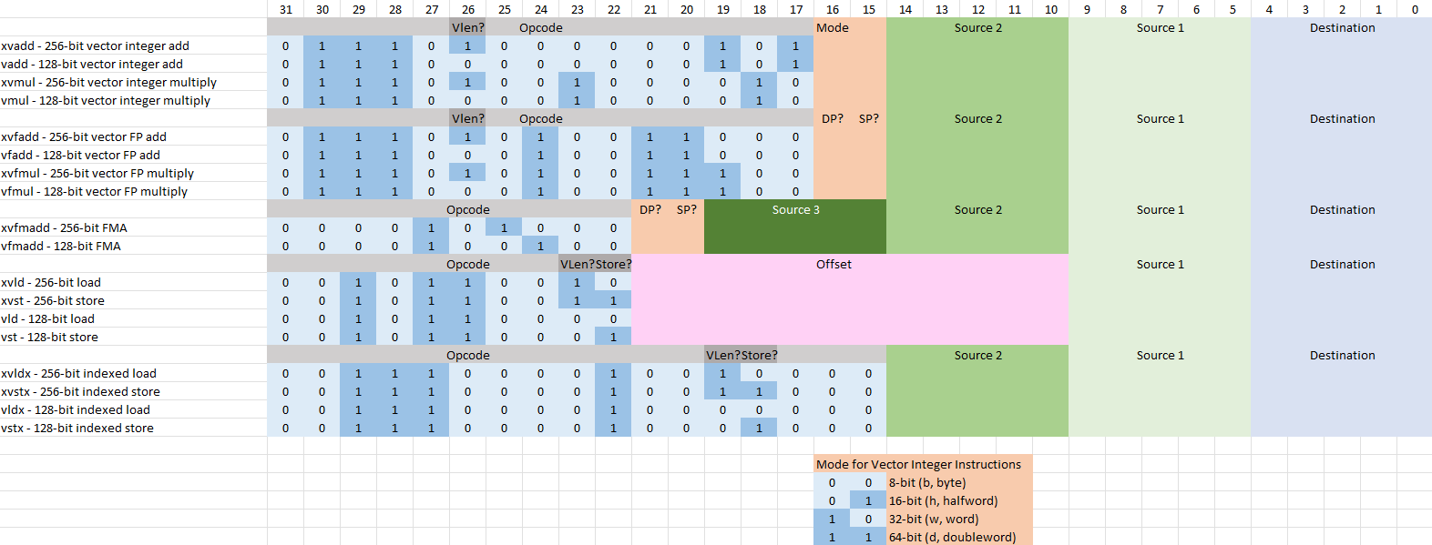
Sometimes, LSX and LASX opcodes differ by a single bit, suggesting that bit indicates whether the instruction targets 128-bit or 256-bit vector length. But that doesn’t apply universally. In some cases, a couple of bits immediately below the opcode seem to specify the data type.
Like later versions of MIPS, Loongarch has indexed load instructions for dealing with arrays. Loongson has incorporated versions of these into its LASX and LSX instruction set extensions. Notably though, Loongarch still doesn’t let you specify a base, index, and scale in one instruction. Both x86 and ARM let you do that, letting them perform array accesses with fewer instructions.
From experimentation, LASX has some weird semantics with regards to partial register access. We’re not going to thoroughly analyze the instruction set, but here are some examples of the weirdness.
Partial Register Access
To start, 128-bit LSX math instructions will operate on the entire 256-bit LASX register. Both VFADD.S (add packed FP32 elements in a 128-bit VR register) and VADD.W (packed addition of 32-bit integers in a 128-bit vector register) will also add to the upper 128-bit half of a 256-bit register. Basically, that means a 128-bit math instruction (VFADD) will behave like its 256-bit equivalent (XVFADD) even though their opcodes are different. Contrast that with x86’s behavior, where a 128-bit operation on 256-bit vector will leave the upper half untouched.

Things get even funnier if you load from memory into a partial register alias. Again, x86 leaves the upper half preserved, though a scalar FP load will zero the high bits of a 128-bit register. With Loongson, what happens to the rest of the register appears to be undefined and quite unpredictable. I find undefined behavior interesting.
Loongson’s Loongarch reference manual says the high 32 bits of a 64-bit FP register are undefined after using FLD.S. FLD.S loads a FP32 value from memory and puts it into the first 32 bits of the target register. The rest of the bits are undefined, but the next 32 bits are usually populated with by the next 32-bit value from memory. That suggests the memory subsystem natively handles accesses at 64-bit granularity, and isn’t meant to go smaller.

What happens above the first 64 bits appears to be completely random. Sometimes elements are zero, sometimes they’re garbage, and sometimes the FLD.S instruction acts as a full 256-bit load.
If we shove FLD.S load up to the end of a 16 KB page, so that loading anything more would cross a page boundary, bits 32 to 63 become very unpredictable too. The most common results are either zero, or loading from the start of the cache line. Sometimes more than one extra element is loaded as well. Less commonly, a few elements are loaded from completely random locations, including valid memory locations in the next page.
The 3A5000 displays similarly weird behavior if we fill a 256-bit register, then try to separately fill the first half with VLD (128-bit vector load). Often, the VLD instruction behaves like XVLD, and loads 256 bits into the entire vector register. If the upper 128-bits are across a page boundary, results again become more random.

The takeaway here is that Loongson’s 3A5000 will remember whether a register is holding a 128-bit or 256-bit value. Once that’s the case, operations the low bits of the vector register will have unpredictable effects on the upper bits. Loongson likely considers the upper bits of a vector register to be undefined after an operation on a subset of the register. In theory, this could improve performance or simplify the design. Some x86 CPUs can incur penalties related to preserving the high bits of a vector register when operating on the lower half. For example, Sandy Bridge can incur a 70 cycle penalty when transitioning to and from a “saved state” designed to preserve the upper half of AVX YMM registers.
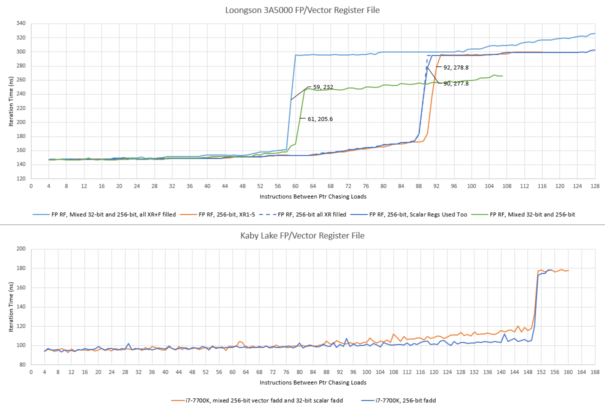
However, Loongson takes a different penalty. If scalar floating point operations are used alongside vector ones, FP/vector renaming capacity decreases by around 32 entries. Even though the registers are aliased to each other (F0-F31 refer to the same architectural registers as XR0-XR31), it looks like the core has to separately store state for both of them. Sandy Bridge has it worse, with FP renaming capacity severely reduced when mixing scalar and vector operations. Newer CPUs like Skylake don’t take any impact to reordering capacity.
3A5000’s Vector Performance
Loongson’s 3A5000 is the only CPU with LSX/LASX support, so we’ll take a look into its FPU and vector implementation here. The 3A5000 has a dual port FPU, with native support for 256-bit execution. Both the execution units and the registers are 256 bits wide. To feed the execution units, the L1D can handle two 256-bit accesses per cycle. Both can be loads, and one can be a store. Unlike on Zen 1, there’s no splitting 256-bit instructions into two 128-bit micro-ops.

Vector integer and logic operations can use both pipes, with simple operations like adds and bitwise operations enjoying single cycle latency. More complicated operations like permutes or integer multiplies take three or four cycles, which is quite decent. For floating point operations, the vector unit is less capable. FP adds and multiplies each get a specialized pipe, creating parallels to Sandy Bridge and older designs. Loongson does have FMA support, but both pipes share a single FMA unit. That setup lets FMA operations dual issue alongside a FP add or FP multiply. However, an even mix of FP add, FP multiply, and FMA instructions doesn’t quite reach 2 IPC, possibly because of sub-optimal pipe assignment and contention for the shared FMA unit.
Floating point execution units tend to be bigger and more power hungry than integer ones. Loongson’s strategy probably focused on getting the benefits of 256-bit vector length rather than going for maximum performance. Floating point throughput matches Zen 1 assuming programs can use 256-bit vectors. But the 3A5000 falls behind Skylake, which can do two 256-bit FMA instructions per cycle. Loongson also struggles with latency. Basic FP operations execute with 5 cycle latency, which is far from ideal especially at a low 2.5 GHz clock speed. For comparison, Zen 1 can execute FP adds and multiplies with 3 cycle latency. FMA operations on Zen 1 have 5 cycle latency.
| Instruction | Description | 3A5000 Throughput/Latency | Pipe? |
| xvadd.d | 256-bit vector add with packed 64-bit integers | 2 per cycle 1 cycle latency |
Both |
| xvmul.d | 256-bit vector multiply with packed 64-bit integers | 2 per cycle 4 cycle latency |
Both |
| xvxor.v | 256-bit bitwise exclusive or | 2 per cycle 1 cycle latency |
Both |
| xvsll.h | 256-bit vector shift | 2 per cycle 1 cycle latency |
Both |
| xvfadd.s | 256-bit vector add with packed FP32 elements | 2 per cycle 5 cycle latency |
FADD pipe |
| xvfmul.s | 256-bit vector multiply with packed FP32 elements | 2 per cycle 5 cycle latency |
FMUL pipe |
| xvfmadd.d | 256-bit vector fused multiply add with packed FP64 elements | 1 per cycle 5 cycle latency |
Both, but only one execution unit |
| xvpermi.d | 256-bit permute, controlled by immediate | 2 per cycle 3 cycle latency |
Both |
Therefore, Loongson doesn’t seem to be aiming particularly high with its vector execution units. The 3A5000 is not going to push through more vector operations per cycle than Zen 1, even though Zen 1 has 128-bit execution units. Its floating point side isn’t very strong, with high latency and low throughput compared to Intel and AMD’s 2017 era technology. Non-FP execution is better, though Intel and AMD can still bring more ports and more throughput to bear.
To hide execution and memory access latency, the 3A5000 has a unified 32 entry FP scheduler and 96 vector registers available for renaming (though with the caveat from above). Add in 32 non-speculative registers, and we’re probably looking at 128 total vector registers. Those registers are 256 bits wide, giving 4 KB of total vector RF capacity. Zen 1 uses a unified 36 entry FP scheduler, with a 64 entry non-scheduling queue in front of it. AMD therefore can track a lot more operations waiting for execution, even if it has to split 256-bit instructions into two micro-ops. Loongson does have a lead with register file capacity, because AMD only has 128-bit wide registers (and 160 of them total). But that advantage will only show if applications use 256-bit vectors a lot.
In terms of execution units and scheduling resources, the 3A5000’s FPU lands somewhere between high performance and low power implementations. It’s not a match for Zen 1, and definitely not a match for Skylake. Loongson’s 256-bit vector width and unified scheduler should give it a leg up over Ampere Altra, but from our libx264 testing, that wasn’t really the case. The 3A5000 does convincingly beat Intel’s old Goldmont Plus based Celeron J4125 in the same video encoding test. However Goldmont Plus aims for a much lower power target than the 3A5000 and Goldmont Plus lacks any AVX or FMA instructions.
Final Words
By using incompatible encodings, Loongson can say they have a new ISA and develop it independently from MIPS. Calling it Loongarch rather than MIPS means they don’t have to deal with rights for the ISA, even if Loongarch and MIPS share a lot of semantics to the point where you can use MIPS64 manuals. This approach makes a lot of sense. Keeping the semantics means Loongson can quickly reuse most of the toolchain. Changing the encodings means they have a new ISA and aren’t held back by any licensing restrictions.
Alongside AVX and SVE, Loongson’s LASX is another ISA extension that takes vector length above 128 bits. More importantly, Loongson is part of China’s efforts to build up domestic CPU capabilities. LASX suggests China is aiming for high performance, because 128-bit vector execution would be adequate for low power applications where high performance is not a concern.
Yet the Loongson 3A5000’s LASX implementation is not competitive with AVX2 implementations found in AMD and Intel desktop CPUs, even if we go back a couple of generations. Skylake and Zen 1 both have wider vector execution setups and can keep more operations in flight to absorb latency. The 3A5000’s low clocks put a giant nail in the coffin, ensuring that it’s completely outmatched by any remotely modern desktop CPU. For sure, getting 256-bit vector execution units to run at high clock speeds is a challenging exercise. But AMD and Intel have figured out how to do it. Loongson has not.
If you like our articles and journalism and you want to support us in our endeavors then consider heading over to our Patreon or our PayPal if you want to toss a few bucks our way or if you would like to talk with the Chips and Cheese staff and the people behind the scenes then consider joining our Discord.